
STK400-030
SANYO Electric Co., Ltd. Semiconductor Business Headquarters
TOKYO OFFICE Tokyo Bldg., 1-10, 1 Chome, Ueno, Taito-ku, TOKYO, 110 JAPAN
N0697HA (ID) No. 5703--1/6
Ordering number: EN 5703
Thick Film Hybrid IC
AF Power Amplifier (Split Power Supply)
(20W+20W+20W, THD = 0.4%)
Overview
The STK400-030 is a 3-channel AF power amplifier IC
supporting multichannel speakers. One package includes
20W
◊
3ch for Lch, Rch and Cch. It is pin compatible with
both 3-channel output devices (STK400-*00 series) and 2-
channel output devices (STK401-*00 series). The output
load impedance is 6/3
.
Features
∑ New series combining 3-channel output devices
(STK400-*00 series) and 2-channel output devices
(STK401-*00 series) with the same pin compatibility.
∑ Output load impedance is 6/3
.
∑ Pin assignment is grouped into individual blocks of
inputs, outputs and supply lines, minimizing the adverse
effects of pattern layout on operating characteristics.
∑ Minimum number of external components required.
Package Dimensions
unit: mm
4086A
Specified Transformer Power Supply
(RP-25 or Equivalent)
[STK400-030]
Specifications
Maximum Ratings
at Ta = 25
∞
C
Operating Characteristics
at Ta = 25
∞
C, R
L
= 6
(noninductive load), Rg = 600
, VG = 40dB
Parameter
Symbol
Conditions
Ratings
Unit
Maximum supply voltage
V
CC
max
±
34
V
Thermal resistance
j-c
Per power transistor
2.1
∞
C/W
Junction temperature
Tj
150
∞
C
Operating substrate temperature
Tc
125
∞
C
Storage temperature
Tstg
-
30 to +125
∞
C
Available time for load short-circuit
t
s
V
CC
=
±
23V, R
L
= 6
,
f = 50Hz, P
O
= 20W
1
s
Parameter
Symbol
Conditions
min
typ
max
Unit
Output power
P
O
(1)
V
CC
=
±
23V, f = 20Hz to
20kHz, THD = 0.4%
20
25
≠
W
P
O
(2)
V
CC
=
±
19V, f = 1kHz,
THD = 1.0%, R
L
= 3
20
25
≠
W
Total harmonic distortion
THD(1)
V
CC
=
±
23V, f = 20Hz to
20kHz, P
O
= 1.0W
≠
≠
0.4
%
THD(2)
V
CC
=
±
23V, f = 1kHz,
P
O
= 5.0W
≠
0.02
≠
%

STK400-030
No. 5703--2/6
Notes.
All tests are conducted using a constant-voltage regulated power supply unless otherwise specified.
Available time for load shorted and output noise voltage are measured using the transformer power supply specified on page 1.
The output noise voltage is the peak value of an average-reading meter with an rms value scale (VTVM). A regulated AC supply (50Hz) should be used to eliminate the
effects of AC primary line flicker noise.
Equivalent Circuit
Sample Application Circuit
Frequency response
f
L
, f
H
V
CC
=
±
23V, P
O
= 1.0W,
≠
20 to 50k
≠
Hz
Input impedance
r
i
V
CC
=
±
23V, f = 1kHz,
P
O
= 1.0W
≠
55
≠
k
Output noise voltage
V
NO
V
CC
=
±
28V, Rg = 10k
≠
≠
1.2
mVrms
Quiescent current
I
CCO
V
CC
=
±
28V
30
90
150
mA
Neutral voltage
V
N
V
CC
=
±
28V
-
70
0
+70
mV
Parameter
Symbol
Conditions
min
typ
max
Unit
+0
-
3
dB
STK400-030
No. 5703--3/6
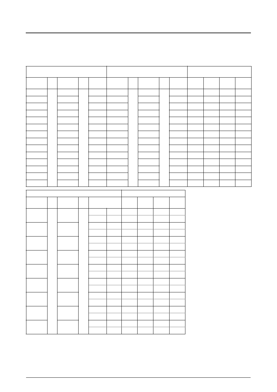
Series Configuration
The products are serialized according to the number of channels, the output capacity, and the distortion ratio. These
include the products under development: for details, please contact your Sanyo sales representative.
V
CC
max1 (R
L
= 6
), V
CC
max2 (R
L
= 3 to 6
), V
CC
1 (R
L
= 6
), V
CC
2 (R
L
= 3
)
STK400-000, STK400-200 series
(3-channel equal output)
STK401-000, STK401-200 series (2-channel)
Supply voltage [V]
Type No.
THD
[%]
Type No.
THD
[%]
Rated
output
Type No.
THD
[%]
Type No.
THD
[%]
Rated
output
V
CC
max1
V
CC
max2
V
CC
1
V
CC
2
STK400-010
0.4
STK400-210
0.08
10W
◊
3
STK401-010
0.4
STK401-210
0.08
10W
◊
2
≠
±
26.0
±
17.5
±
14.0
STK400-020
STK400-220
15W
◊
3
STK401-020
STK401-220
15W
◊
2
≠
±
29.0
±
20.0
±
16.0
STK400-030
STK400-230
20W
◊
3
STK401-030
STK401-230
20W
◊
2
≠
±
34.0
±
23.0
±
19.0
STK400-040
STK400-240
25W
◊
3
STK401-040
STK401-240
25W
◊
2
≠
±
36.0
±
25.0
±
21.0
STK400-050
STK400-250
30W
◊
3
STK401-050
STK401-250
30W
◊
2
≠
±
39.0
±
26.0
±
22.0
STK400-060
STK400-260
35W
◊
3
STK401-060
STK401-260
35W
◊
2
≠
±
41.0
±
28.0
±
23.0
STK400-070
STK400-270
40W
◊
3
STK401-070
STK401-270
40W
◊
2
≠
±
44.0
±
30.0
±
24.0
STK400-080
STK400-280
45W
◊
3
STK401-080
STK401-280
45W
◊
2
≠
±
45.0
±
31.0
±
25.0
STK400-090
STK400-290
50W
◊
3
STK401-090
STK401-290
50W
◊
2
≠
±
47.0
±
32.0
±
26.0
STK400-100
STK400-300
60W
◊
3
STK401-100
STK401-300
60W
◊
2
≠
±
51.0
±
35.0
±
27.0
STK400-110
STK400-310
70W
◊
3
STK401-110
STK401-310
70W
◊
2
±
56.0
≠
±
38.0
≠
≠
≠
≠
STK401-120
STK401-320
80W
◊
2
±
61.0
≠
±
42.0
≠
≠
≠
≠
STK401-130
STK401-330
100W
◊
2
±
65.0
≠
±
45.0
≠
≠
≠
≠
STK401-140
STK401-340
120W
◊
2
±
74.0
≠
±
51.0
≠
STK400-400, STK400-600 series (3-channel different output)
Supply voltage [V]
Type No.
THD
[%]
Type No.
THD
[%]
Rated output
V
CC
max1
V
CC
max2
V
CC
1
V
CC
2
STK400-450
0.4
STK400-650
0.08
Cch
30W
≠
±
39.0
±
26.0
±
22.0
L, Rch
15W
≠
±
29.0
±
20.0
±
16.0
STK400-460
STK400-660
Cch
35W
≠
±
41.0
±
28.0
±
23.0
L, Rch
15W
≠
±
29.0
±
20.0
±
16.0
STK400-470
STK400-670
Cch
40W
≠
±
44.0
±
30.0
±
24.0
L, Rch
20W
≠
±
34.0
±
23.0
±
19.0
STK400-480
STK400-680
Cch
45W
≠
±
45.0
±
31.0
±
25.0
L, Rch
20W
≠
±
34.0
±
23.0
±
19.0
STK400-490
STK400-690
Cch
50W
≠
±
47.0
±
32.0
±
26.0
L, Rch
25W
≠
±
36.0
±
25.0
±
21.0
STK400-500
STK400-700
Cch
60W
≠
±
51.0
±
35.0
±
27.0
L, Rch
30W
≠
±
39.0
±
26.0
±
22.0
STK400-510
STK400-710
Cch
70W
±
56.0
≠
±
38.0
≠
L, Rch
35W
≠
±
41.0
±
28.0
±
23.0
STK400-520
STK400-720
Cch
80W
±
61.0
≠
±
42.0
≠
L, Rch
40W
≠
±
44.0
±
30.0
±
24.0
STK400-530
STK400-730
Cch
100W
±
65.0
≠
±
45.0
≠
L, Rch
50W
≠
±
47.0
±
32.0
±
26.0
STK400-030
No. 5703--4/6
Heatsink Design Considerations
The heatsink thermal resistance,
c-a, required to cover
the hybrid IC's total power dissipation, Pd, is determined
as follows:
Condition 1: Hybrid IC's substrate temperature not to
exceed 125
∞
C.
Pd
◊
c-a + Ta < 125
∞
C ........................................ (1)
where Ta is the guaranteed maximum ambient tempera-
ture.
Condition 2: Power transistor junction temperature, Tj, not
to exceed 150
∞
C.
Pd
◊
c-a + Pd/N
◊
j-c + Ta < 150
∞
C ................. (2)
where N is the number of power transistors and
j-c is the
thermal resistance per power transistor. Note that the
power dissipated per transistor is the total, Pd, divided
evenly among the N power transistors.
Expressions (1) and (2) can be rewritten making
c-a the
subject.
c-a < (125
-
Ta)/Pd ............................................. (1)
c-a < (150
-
Ta)/Pd
-
j-c/N .............................. (2)
The heatsink required must have a thermal resistance that
simultaneously satisfies both expressions.
The heatsink thermal resistance can be determined from
(1)
and (2)
once the following parameters have been
defined.
∑ Supply voltage
: V
CC
∑ Load resistance
: R
L
∑ Guaranteed maximum ambient temperature
: Ta
The total device power dissipation when hybrid IC's V
CC
=
±
23V and R
L
= 6
, for a continuous sine wave signal, is
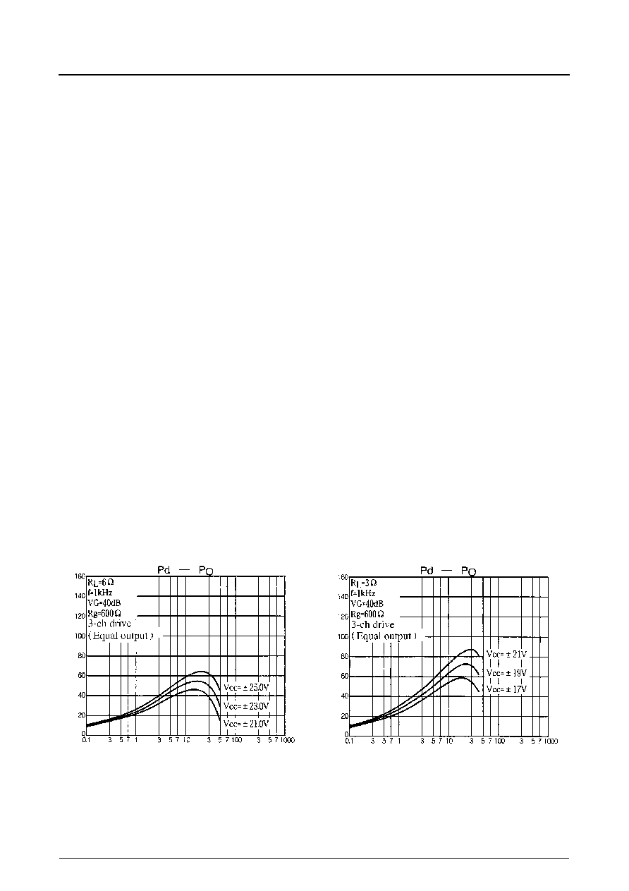
a maximum of 55W, as is in Pd-P
O
graph.
When estimating the power dissipation for an actual audio
signal input, the rule of thumb is to select Pd correspond-
ing to 1/10 P
O
max (within safe limits) for a continuous
sine wave input. For example,
Pd = 31W (for 1/10 P
O
max = 2W)
The hybrid IC has 6 power transistors, and the thermal
resistance per transistor,
j-c, is 2.1
∞
C/W. If the guaran-
teed maximum ambient temperature, Ta, is 50
∞
C, then the
required heatsink thermal resistance,
c-a, is:
From expression (1)
:
c-a < (125
-
50)/31
< 2.41
From expression (2)
:
c-a < (150
-
50)/31
-
2.1/6
< 2.87
Therefore, to satisfy both expressions, the required heat-
sink must have a thermal resistance less than 2.41
∞
C/W.
Similarly, when hybrid IC's V
CC
=
±
19V and R
L
= 3
:
Pd = 36W (for 1/10 P
O
max = 2W)
From expression (1)
:
c-a < (125
-
50)/36
< 2.08
From expression (2)
:
c-a < (150
-
50)/36
-
2.1/6
< 2.42
Therefore, to satisfy both expressions, the required heat-
sink must have a thermal resistance less than 2.08
∞
C/W.
This heatsink design example is based on a constant-volt-
age egulated power supply, and should be verified within
your specific set environment.
Output power per channel, P
O
/ch - W
3-ch dri
v
e, total de
vice po
wer dissipation, Pd -
W
Output power per channel, P
O
/ch - W
3-ch dri
v
e, total de
vice po
wer dissipation, Pd -
W
STK400-030
No. 5703--5/6
Output power, P
O
- W
Input voltage, Vin - mVrms
Supply voltage, V
CC
- V
T
otal harmonic distortion,
THD - %
Output po
wer
, P
O
-
W
Output po
wer
, P
O
-
W
Output power, P
O
- W
Frequency, f - Hz
Frequency, f - Hz
T
otal harmonic distortion,
THD - %
Output po
wer
, P
O
-
W
Open-Loop Gain,
V
G
- dB
STK400-030
No. 5703--6/6
s
No products described or contained herein are intended for use in surgical implants, life-support systems, aerospace equipment, nuclear
power control systems, vehicles, disaster/crime-prevention equipment and the like, the failure of which may directly or indirectly cause injury,
death or property loss.
s
Anyone purchasing any products described or contained herein for an above-mentioned use shall:
Accept full responsibility and indemnify and defend SANYO ELECTRIC CO., LTD., its affiliates, subsidiaries and distributors and all their
officers and employees, jointly and severally, against any and all claims and litigation and all damages, cost and expenses associated
with such use:
Not impose any responsibility for any fault or negligence which may be cited in any such claim or litigation on SANYO ELECTRIC CO.,
LTD., its affiliates, subsidiaries and distributors or any of their officers and employees, jointly or severally.
s
Information (including circuit diagrams and circuit parameters) herein is for example only; it is not guaranteed for volume production. SANYO
believes information herein is accurate and reliable, but no guarantees are made or implied regarding its use or any infringements of
intellectual property rights or other rights of third parties.
This catalog provides information as of November, 1997. Specifications and information herein are subject to change without notice.
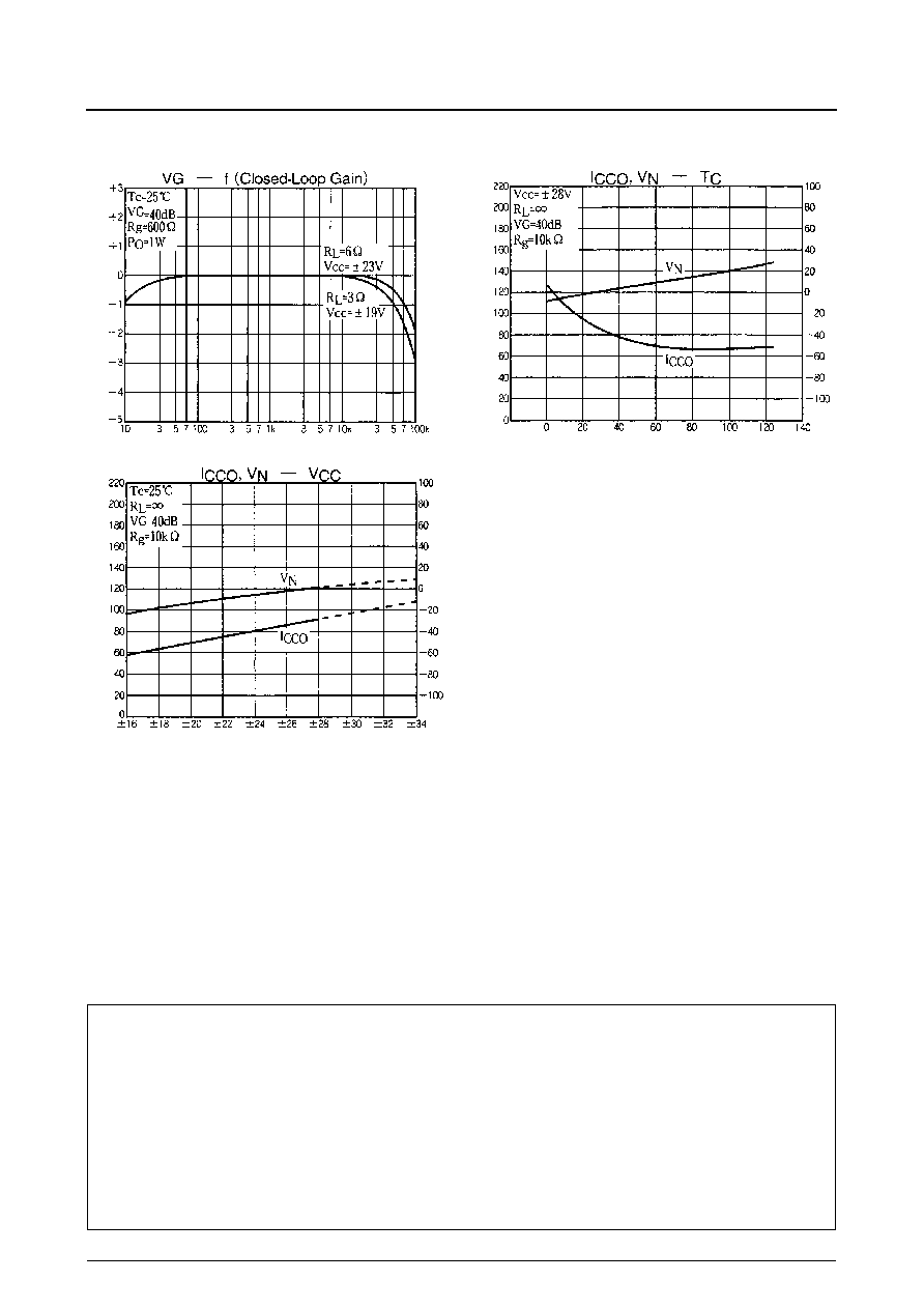
Frequency, f - Hz
Supply voltage, V
CC
- V
Closed-Loop Gain,
V
G
- dB
Quiescent current, I
CCO
- mA
Neutral v
oltage,
V
N
- mV
Operating substrate temperature, Tc -
∞
C
Quiescent current, I
CCO
- mA
Neutral v
oltage,
V
N
- mV